When the first edition of Gear Shift went out on April 11, the story was about funding ambition — ₹1.2 lakh crore committed, ISM 2.0 announced, the DHRUV64 chip making its debut. Two weeks later, the story is about geography.
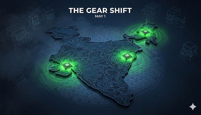
India’s semiconductor map is no longer a Gujarat story. In the fortnight since our last roundup, a groundbreaking happened in Bhubaneswar, a Special Economic Zone was notified in Dholera, and a strategic technology pact with the United States moved from policy dialogue to industrial execution. Taken together, these developments tell you something important: the infrastructure for chip production is now being planted across six states — and one of them is Assam.
Here is what happened, and why it matters for manufacturers in the Northeast.
Story 1: Odisha Becomes India’s Most Advanced Semiconductor State
On April 19, the foundation stone was laid at Info Valley in Bhubaneswar for India’s first advanced 3D glass substrate semiconductor packaging unit. The project — led by US-based 3D Glass Solutions through its Indian subsidiary, Heterogeneous Integration Packaging Solutions Pvt Ltd (HIPSPL) — involves an investment of ₹1,943 crore and is being implemented under the India Semiconductor Mission. The official PIB release and The Week’s coverage have the full details.
The technology itself is worth understanding. Conventional chip packaging stacks components using organic substrates. Advanced 3D glass packaging instead uses glass as the base material, stacking multiple chips together to dramatically improve performance while shrinking size and reducing power consumption. Until now, no facility in India could do this at commercial scale. Once this plant reaches full operation (commercial production is targeted for August 2028, full-scale by August 2030), it will produce 50 million assembled units and approximately 13,000 advanced 3D heterogeneous integration modules per year.
The sectors it will serve are worth noting: artificial intelligence, 5G/6G communications, data centres, defence electronics, automotive radar, and aerospace. This is not consumer electronics — this is the hardware that powers strategic infrastructure.
What makes the Odisha story particularly significant is the double milestone. Odisha now hosts both the country’s first compound semiconductor fabrication unit (being built by SiCSem) and the first 3D glass substrate packaging facility — both on the same industrial campus at Info Valley, Khordha. No other state in India has this combination.
The Centre is supporting the HIPSPL project with ₹799 crore in fiscal assistance, and the Odisha state government is adding approximately ₹399.5 crore — together covering nearly 60% of the project cost. Lip-Bu Tan, the Intel CEO, participated virtually at the groundbreaking ceremony, and the names associated with this technology — Intel, Lockheed Martin, Applied Materials — tell you what tier of the global supply chain is now watching India’s packaging sector.
The MSME angle: Advanced packaging facilities like this one generate substantial demand for ancillary services — precision cleaning, specialty chemicals, inert gas handling, logistics for fragile components, and facility maintenance. The procurement ramp-up period, typically 18–24 months before commercial production begins, is exactly when MSME vendors in supporting states should be qualifying their capabilities.
Story 2: India’s First Chip Fab Gets Its Legal Foundation
Three days before our last edition, on April 9, the central government notified the Special Economic Zone for Tata Semiconductor Manufacturing Pvt Ltd in Dholera, Gujarat. This is not just a procedural step. The SEZ notification formalises the regulatory framework for India’s first semiconductor fabrication facility — the plant that will actually manufacture chips using front-end processes, not just assemble or test them. India Briefing has a useful explainer on the full SEZ cluster that puts the Dholera notification in context.
The project spans 66.166 hectares and is expected to generate nearly 21,000 jobs. The Dholera fab sits within a cluster that now includes the Micron ATMP facility (investment: ₹13,000 crore) and the Kaynes Semicon OSAT plant (inaugurated on March 31, with a capacity of 6 million chips per day) — making Sanand-Dholera the highest-concentration semiconductor cluster India has ever assembled.
The SEZ was enabled by a regulatory reform from June 2025 that reduced the minimum land requirement for semiconductor and electronics SEZs from 50 hectares to 10 hectares. That change, which received little coverage at the time, is what allowed smaller players — Kaynes, CG Semi, and others — to also establish dedicated zones.
For context on where this fits in the national picture: as of March 2026, 10 semiconductor units have been approved under the ISM, spanning six states, with cumulative investments exceeding ₹1.60 lakh crore. Of the 10 approved units, two are fabrication plants. The Dholera fab is one of them.
| Facility | State | Type | Investment |
|---|---|---|---|
| Tata Dholera Fab | Gujarat | Fabrication | ₹91,000 Crore |
| Micron ATMP | Gujarat | Assembly, Test, Packaging | ₹13,000 Crore |
| Kaynes Semicon | Gujarat | OSAT | ₹3,300 Crore |
| HIPSPL (3D Glass Solutions) | Odisha | Advanced Packaging | ₹1,943 Crore |
| SiCSem | Odisha | Compound Semiconductor Fab | Undisclosed |
| Tata OSAT (TSAT) | Assam | Assembly, Test | ₹27,000 Crore |
Story 3: The TRUST Framework — What the US-India Pact Actually Means for Chips
The US-India trade deal announced in February 2026 — which lowered the US reciprocal tariff on Indian goods from an effective 50% to 18% — has been well-covered. What has received less attention is the technology architecture embedded within it. The White House fact sheet and the joint statement are the primary sources; Lemonn’s analysis has a readable breakdown of the TRUST framework specifically.
The deal introduces a framework called TRUST: Transforming the Relationship Utilizing Strategic Technology. It replaces the earlier iCET (Initiative on Critical and Emerging Technology) and shifts the relationship from policy dialogue to industrial execution. The practical implications for semiconductors are concrete:
- A national-security fabrication line producing gallium nitride and silicon carbide chips, with US investment from Micron and Applied Materials
- Joint alignment on export controls and inbound/outbound investment reviews
- India’s Semiconductor Mission 2.0 positioned as the domestic counterpart to US chip infrastructure funding
- Bilateral digital trade rules that address barriers to technology product flows
The specific carve-out matters: under the deal, semiconductors were exempted from the initial tariff pressure that hit textiles, chemicals, and auto parts. That exemption reflects a deliberate US interest in keeping India’s chip supply chain accessible — and it gives Indian OSAT and packaging operators a competitive floor that did not exist twelve months ago.
For manufacturers in the Northeast, the TRUST framework has a secondary implication. The chips coming out of Jagiroad are intended, in part, for export to automobile industries in Japan, the United States, and Germany. That export positioning depends on India maintaining a predictable tariff relationship with the US. The trade deal, for all its complexity, provides that floor.
Story 4: Jagiroad — Where Does Phase 1 Stand?
The Tata Semiconductor Assembly and Test (TSAT) facility at Jagiroad, Morigaon, was targeted for Phase 1 commissioning by April 2026. As of this writing, no official production launch announcement has been made, though construction at the 550-acre site was reported as progressing toward completion in late 2025. The PIB press note from December 2025, when a Telangana media delegation visited the facility, has the most recent on-the-record project status.
What we do know from the public record: the project involves an investment of ₹27,000 crore, a designed capacity of 48 million chips per day, and an employment projection of 15,000 direct and 11,000–13,000 indirect jobs. Finance Minister Nirmala Sitharaman reviewed the project on-site in November 2025, accompanied by Chief Minister Himanta Biswa Sarma. Project Head Ashish Mishra confirmed at a December 2025 media interaction that the facility is designed to serve both domestic and global customers.
The commissioning timeline — even if it slips by a quarter or two — does not diminish the structural significance of what is being built at Jagiroad. What was a decommissioned paper mill a decade ago is now the anchor facility for semiconductor manufacturing in Northeast India. The question for local MSMEs is not whether the plant will run — it will — but whether the local vendor ecosystem will be ready when procurement opens.
A useful reference point: when the Kaynes Semicon plant in Sanand ramped up, the immediate requirement was for logistics operators, facility maintenance vendors, packaging material suppliers, and precision cleaning services. None of these require semiconductor expertise. They require documentation, quality systems, and the ability to pass an OEM vendor audit.
ISM 2.0 Mechanics: What the ₹8,000 Crore Actually Funds
The Union Budget 2026–27 allocated a total financial outlay of ₹8,000 crore to the Modified Programme for Development of Semiconductor and Display Manufacturing Ecosystem in India — the operational vehicle for ISM 2.0. The MeitY/PIB programme summary outlines the priorities in full; the programme priorities, as outlined by MeitY, are:
- Semiconductor equipment and materials manufacturing in India (a significant shift — earlier phases focused on fabs and packaging, not the upstream equipment supply chain)
- Full-stack Indian semiconductor intellectual property and chip design
- Industry-led research and training centres
- Advanced manufacturing, with a roadmap defined toward 3-nanometre and 2-nanometre technology nodes by 2035
The equipment and materials focus is the most underreported element. India currently imports virtually all semiconductor manufacturing equipment — the tools that deposit, etch, and measure chip layers. Building a domestic equipment industry is a decade-long project, but the funding signal in ISM 2.0 is that the government has identified it as a gap worth addressing. For MSMEs with precision engineering capabilities — particularly in Assam and the broader Northeast — this creates a pathway that did not formally exist under ISM 1.0.
The 2029 target embedded in ISM 2.0 is to achieve domestic design and manufacture capability for 70–75% of India’s chip requirements across consumer appliances, industrial electronics, automobiles, telecommunications, aerospace, and power electronics.
What This Means for Northeast MSMEs
The pattern across these four stories is the same: investment decisions are being made now, facility construction is underway, and the procurement windows — when vendors actually get qualified and onboarded — will open in the next 12–36 months.
Northeast India has a specific position in this map. Jagiroad is the only OSAT facility in the entire eastern half of the country. When it reaches operational scale, it will require vendors across a range of non-semiconductor categories: construction and civil maintenance, logistics and secure transport, specialty gases and chemicals, facility services, and administrative support. The geographic position of Assam — and the infrastructure improvements at Jogighopa and Pandu — means the logistics corridors to supply that facility are already being built.
The next edition of Gear Shift will track the Tata Jagiroad commissioning announcement, ISM 2.0’s first equipment scheme applications, and any developments on the pending UNNATI scheme renewal — which remains the most directly relevant subsidy instrument for MSMEs in this region.
Gear Shift is a fortnightly roundup of India’s manufacturing and industrial policy developments, with a focus on implications for MSMEs in Northeast India. Published by Nitisagar Advisory, Guwahati. To receive the next edition, visit nitisagar.com.