Assam Is Building a ₹27,000 Crore Chip Plant. This Is The Ecosystem It Needs To Run
Jagiroad's packaging plant can assemble 48 million chips a day, but the leadframes, bonding wire and moulding compound it runs on barely exist in India yet. This report maps what's missing, piece by piece, and which parts an Assam MSME could realistically build.
0 of 6 sections read
Ask most people about India’s semiconductor push and they will describe Dholera. A ₹91,000 crore fab rising out of Gujarat’s coastal flats. India’s first attempt at making chips from raw silicon.
Almost nobody mentions Jagiroad.
That is a mistake, and not just a naming one. Tata Semiconductor Assembly and Test (TSAT), the facility actually under construction in Assam, is not a fab. It is a packaging plant.
The numbers are real regardless of which facility gets the headlines. TSAT represents roughly ₹27,000 crore of investment on a 171-acre campus in Morigaon district, with design capacity to assemble up to 48 million chips a day (Trade Brains, government incentive report).
The difference matters more than it sounds. A fab transforms raw silicon into patterned dies through hundreds of chemical and thermal steps. TSAT does something else entirely.
It takes dies made elsewhere and turns them into shippable chips through mechanical, thermal and electrical assembly. That distinction decides which ancillary industries actually matter to Morigaon.
It is why this report is built around TSAT’s own process chain, not Dholera’s much heavier fab inputs.
The number that matters most
Six of TSAT’s nine core ancillary components are a real, fundable MSME business today: ₹1.5-4.5 crore, 12-18 months, no exotic technology barrier. The other three need a partner, not a founder.
Our earlier analysis of Penang, Sanand and Morigaon built a readiness matrix by urgency. It sorted ancillary industries into what TSAT needs before Day 1, what can wait three years, and what belongs to a longer horizon.
This report asks a different question of the same facts. What actually happens on TSAT’s assembly floor, step by step? And what would each step genuinely cost an Assam MSME to supply?
The headline finding sharpens under this lens. TSAT’s three confirmed platforms, Wire Bond, Flip Chip and Integrated Systems Packaging (ISP), pull on a materials list that is shorter, cheaper to enter, and far more forgiving of import dependency than a fab’s.
- Most of it is genuinely within MSME reach: ₹1.5-4.5 crore, 12-18 months.
- A smaller set, chiefly bonding wire and advanced substrates, is not MSME-buildable at any realistic scale, and should stop being framed as if it were.
Section 2 walks the process floor itself. Section 4 scores all nine components against both tests: how much it hurts if the input is missing, and what it would actually take an MSME to build.
The OECD’s 2025 mapping of the global semiconductor value chain names three process steps: design, front-end fabrication, and “assembly, test and packaging” or ATP, also called back-end manufacturing (OECD, 2025).
TSAT falls entirely inside that third category. Wafers arrive already processed. Each die is cut, packaged into a protective shell, tested and shipped.
It does not fabricate anything. It assembles, connects, protects and verifies.
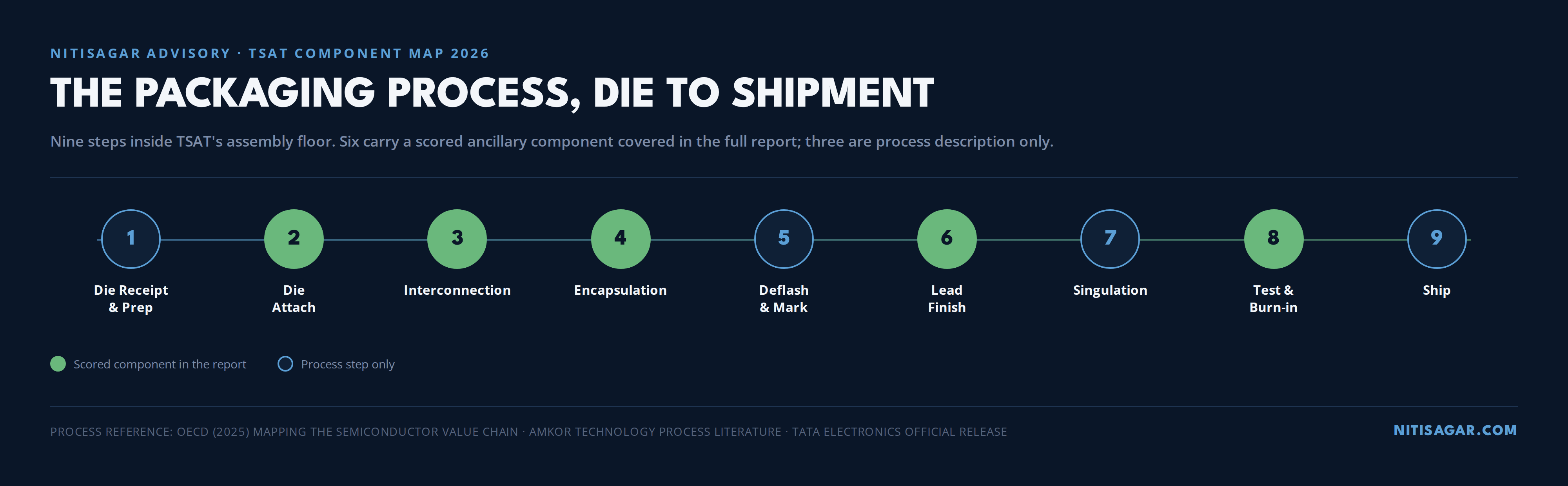
Tata Electronics has confirmed three platform technologies for Jagiroad: Wire Bond, Flip Chip, and Integrated Systems Packaging (ISP), with a roadmap toward more advanced packaging in future (Tata Group, official release).
That trio maps cleanly onto the OECD paper’s own packaging categories: wire bonding, flip chip, wafer-level packaging, system-in-package and 3D packaging. ISP is TSAT’s system-in-package offering.
Nine steps, three sources. The process below draws on OECD’s value-chain framing, Amkor Technology’s published process literature (Amkor is one of the world’s largest OSATs), and an academic literature review of wire bond, flip chip and encapsulation technology.
1. Die receipt and preparation. Wafers processed at a fab elsewhere arrive at TSAT, are mounted, thinned by backgrinding if required, and diced into individual dies using saw or plasma dicing. Key consumables: dicing saw blades, dicing tape and frame.
2. Die attach. Each die is bonded to a leadframe or substrate, either with epoxy adhesive or film die-attach, or with solder for flip-chip formats. A wire-bond, die-up QFN package is prepared by attaching the leadframe to adhesive tape, then adhering the die by thermo-compression (Amkor patent literature, USPTO). Key inputs: leadframes, substrates, die-attach adhesive or film.
3. Interconnection - the platform fork. This is where Wire Bond, Flip Chip and ISP genuinely diverge.
- Wire Bond: the die is electrically connected to the lead terminals by wire bonding, using fine gold or copper wire, ball or wedge bonded (Amkor, USPTO patent literature).
- Flip Chip: the die, already bumped with solder balls, is flipped and bonded face-down onto the substrate through the bumps, with underfill dispensed to fill the gap. A typical wire-bond connection carries roughly 1 nH of inductance per millimetre, against as little as 50 pH for a bump bond, a real difference for high-speed and automotive applications (Fermilab, arXiv).
- ISP: combines elements of both, integrating multiple dies and passive components onto a single substrate.
4. Encapsulation. The leadframe or substrate, with die and interconnects attached, is placed into a multi-cavity mould. Epoxy moulding compound (EMC) is heated and pressed in to form the protective package body (SemiconductorX, industry process reference).
5. Post-mould cure, deflash and mark. The moulded package is cured, excess mould flash is removed, and the package is laser-marked for permanent identification and traceability.
6. Lead finish and plating. For leadframe-based packages, exposed leads or pads are plated, commonly with a tin-based finish, to ensure solderability when the finished chip is later mounted onto a customer’s circuit board.
7. Singulation. Individual packages are separated from the leadframe strip or substrate panel, by saw or by punch.
8. Test and burn-in. Each packaged chip is electrically tested. Automotive-grade programmes typically add burn-in and extended reliability testing, given the zero-defect and zero-delamination expectations automotive customers hold OSAT suppliers to (Amkor, automotive leadframe packaging literature).
9. Finished-goods packaging and shipment. Tested chips are packed, typically in tape-and-reel or moisture-barrier bagging with desiccant, and shipped to the OEM or to a board-assembly facility.
A note on terminology
Our earlier cluster analysis used “ISIP” (Integrated System-in-Package) for TSAT’s third platform. Tata Electronics’ own press materials use “Integrated Systems Packaging (ISP).” We use ISP here as the primary-source term, without meaning to contradict the earlier report - both refer to the same offering.
Six of these nine steps carry a scored ancillary component. The other three, dicing, deflash and mark, and shipment, are process description only.
Section 4 scores each of those six, plus three cross-cutting inputs, two ways: what breaks if the component is missing, and what it would cost an MSME to build.
The full nine-step process is also built as a clickable diagram, embedded directly below.
Click any stage to expand it, click any component pill for its best-case and worst-case detail, and use the platform toggle to compare how Wire Bond, Flip Chip and ISP diverge at the interconnection step.
(This interactive version only works online.)
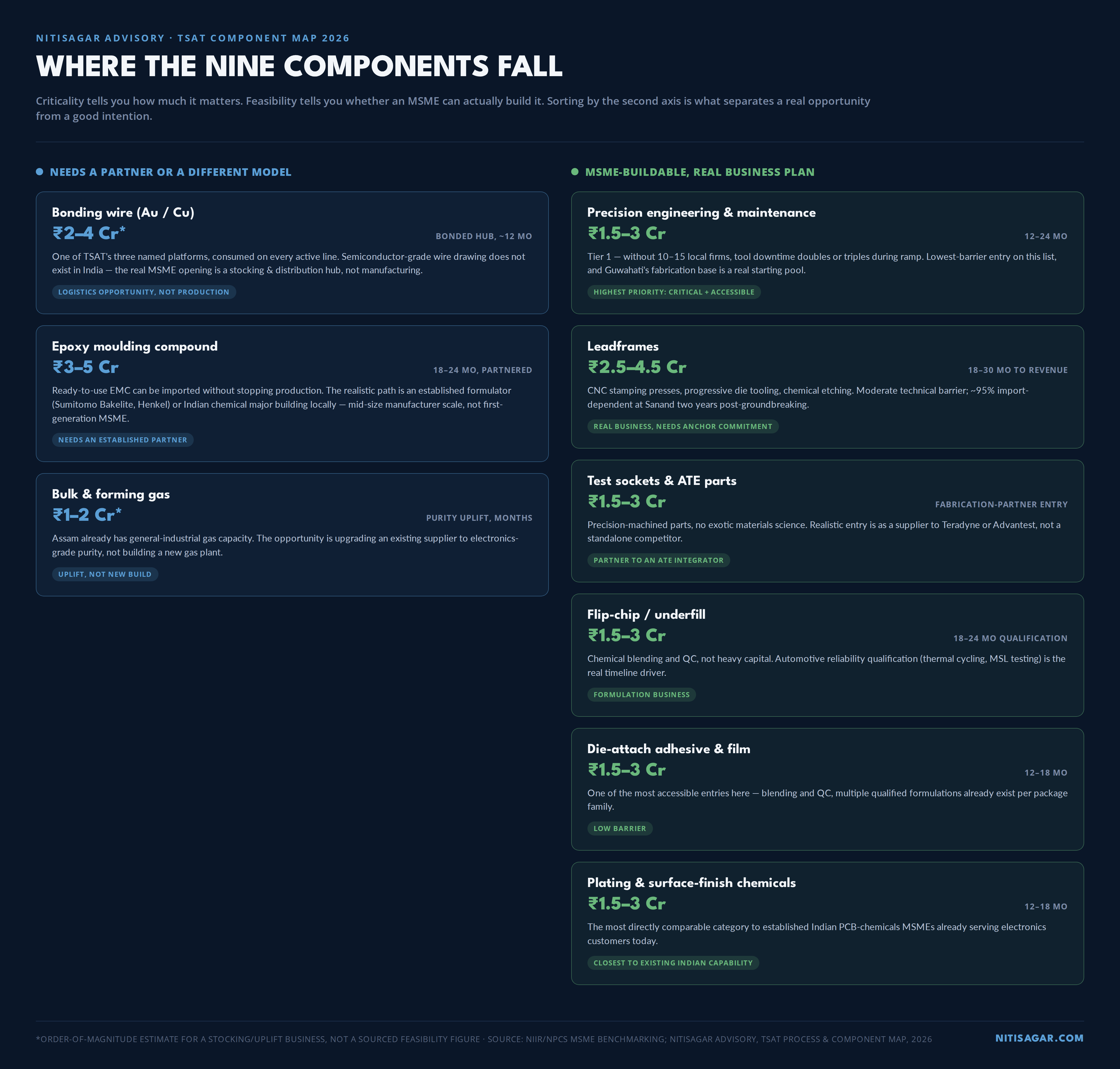
Where each component falls, at a glance:
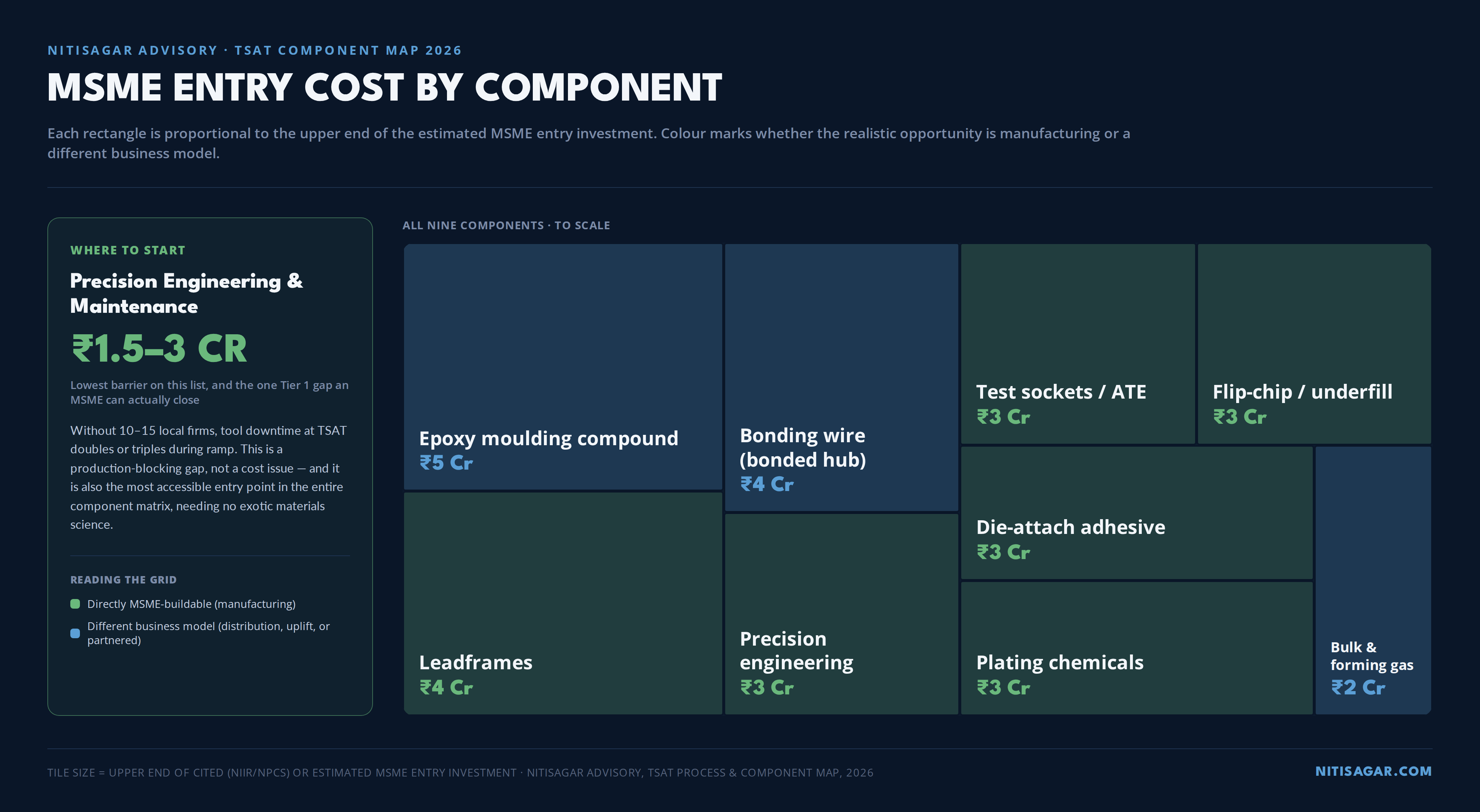
What it costs to get in:
Two questions matter for each component, and they are not the same question.
- Operational: what actually happens at TSAT if this input is unavailable or delayed?
- Entrepreneurial: what would it genuinely take an Assam-based MSME to start supplying it?
A component can be highly critical and still be a poor MSME opportunity. Bonding wire is that case.
A component can also be moderately critical and an excellent MSME opportunity. Leadframes are closer to that. The full pattern across all nine appears in Section 5.
How the scoring works, in both columns:
- Best case - import dependency is manageable, a cost and lead-time problem only.
- Realistic case - grounded in the cost premiums and timelines from our Sanand and Morigaon readiness matrix.
- Worst case - a genuine production or quality stoppage.
MSME entry gets the same three-point range: investment, timeline, and the realistic ceiling on what an entrant can achieve without a large-player partner.
On the investment figures
MSME entry costs draw on NIIR/NPCS’s India Semiconductor MSME Business Ideas benchmarking. Treat these as feasibility-report-style industry estimates, not audited figures, and verify against a current techno-economic feasibility study before committing capital.
1. Leadframes
Process step: Die attach. Platform: Wire Bond primarily, also some ISP formats.
Leadframes are precision-stamped or etched copper-alloy or iron-nickel-alloy sheets that carry the die and provide the electrical path outward. India currently imports most of its requirement.
| Scenario | Criticality if missing | MSME entry |
|---|---|---|
| Best case | Tier 2, not production-stopping with multi-vendor sourcing and buffer stock. Import cost ₹800-1,200/unit vs ₹600-800 in Penang - a cost penalty, not a stoppage. | ₹2.5-4.5 Cr for CNC stamping presses, progressive die tooling, chemical etching and surface-treatment lines. Moderate technical barrier (NIIR/NPCS). |
| Realistic case | ~95% import dependency at Sanand two years after groundbreaking. Est. ₹300-500 Cr/year premium at TSAT’s volume; 75-90 day procurement cycle from Japan. | 12-18 months to first shipment, plus 6-12 months of AEC-Q/JEDEC qualification. Time-to-revenue: 18-30 months. |
| Worst case | Package-specific tooling, not interchangeable across families. A supply shock with no second source halts that line until requalification, itself months long. | Finer-pitch automotive formats push capital past ₹4.5 Cr and need metallurgical expertise scarcer here than in Gujarat’s auto-ancillary base. Needs a TSAT purchase commitment to justify speculative capacity. |
2. Bonding wire (gold and copper)
Process step: Interconnection. Platform: Wire Bond primarily; also used within ISP formats, which combine wire bond and flip-chip interconnects on one substrate.
| Scenario | Criticality if missing | MSME entry |
|---|---|---|
| Best case | A bonded-warehouse buffer turns 100% import dependency into a working-capital problem, cutting exposure from 75-90 days to 7-14. | A HAZMAT-rated bonded stocking hub, no wire-drawing tech needed, is achievable in ~12 months for a few crore in warehouse fit-out and working capital. |
| Realistic case | 15-20% price premium on freight alone. No domestic wire drawing or heat treatment anywhere in India; consumed continuously on every line. | Actual wire drawing for semiconductor-grade wire does not exist in India. Even the start of domestic drawing is 30-36 months out, nationally. |
| Worst case | Wire Bond is one of three named platforms, not a peripheral one. A sustained outage stops an entire packaging platform at once. | Bonding wire has some of the tightest purity and pull-strength tolerances in OSAT. An MSME attempting wire-drawing from scratch would almost certainly fail qualification. |
The honest takeaway on bonding wire
This is the clearest case in the matrix: genuinely critical, genuinely not an MSME manufacturing opportunity. The real opening is logistics and stocking, not production.
Framing bonding-wire manufacturing as an MSME target sets founders up against a qualification barrier a garage-to-scale entrant cannot clear.
3. Flip-chip interconnect: solder bumps and underfill
Process step: Interconnection. Platform: Flip Chip specifically, also used within ISP.
| Scenario | Criticality if missing | MSME entry |
|---|---|---|
| Best case | Dies typically arrive pre-bumped from the fab or a bumping house. Exposure here is mainly to underfill, lower-volume and more substitutable than bonding wire. | Underfill and flux chemistries fall in the ₹1.5-3 Cr specialty-formulation bracket - blending and QC, not heavy capital (NIIR/NPCS). |
| Realistic case | Flip chip’s ~1 nH/mm inductance vs ~50 pH for a bump bond (arXiv/Fermilab) is why it’s a named TSAT platform. Underfill quality drives thermal-cycling reliability, which matters acutely for automotive customers. | 18-24 months from formulation to a qualified automotive-grade shipment, matching Sanand’s timeline for encapsulation-adjacent chemistries. |
| Worst case | Underfill voiding or delamination is a latent defect: passes test, fails in the field. The most damaging outcome for an automotive supplier. | Advanced wafer-level bumping needs cleanroom-grade process control closer to fab economics. Not realistically MSME-feasible - a JV or large-player category. |
4. Epoxy moulding compound (EMC)
Process step: Encapsulation. Platform: All three.
| Scenario | Criticality if missing | MSME entry |
|---|---|---|
| Best case | Ready-to-use EMC can be imported. Tier 2, not Tier 1 - raises cost, doesn’t stop production, as long as supply holds. | ₹3-5 Cr, 15-22% margin, for a compounding operation under license or in partnership with an established formulator (NIIR/NPCS). |
| Realistic case | ~90% import dependency at Sanand scale means an est. ₹50-100 Cr/year premium at TSAT’s volume, and limits customisation for ISP and flip-chip packages. | Realistic pathway is an established firm (Sumitomo Bakelite, Henkel) or Indian chemical company building a unit within 18-24 months - mid-size manufacturer scale, not first-gen MSME. |
| Worst case | Unlike bonding wire, EMC can’t be pulled from a generic buffer - different packages need different rheology. A disruption stalls encapsulation for that whole package family. | Formulating EMC from first principles needs filler chemistry and rheology R&D - a multi-year build with no credible domestic-only pathway. |
5. Die-attach adhesives and film die-attach
Process step: Die attach. Platform: All three; film die-attach favoured for automotive programmes.
| Scenario | Criticality if missing | MSME entry |
|---|---|---|
| Best case | Standard epoxy paste is lower-volume, less exotic chemistry than EMC or bonding wire, with multiple qualified formulations usually available. | Falls squarely in the ₹1.5-3 Cr PCB/specialty-chemicals bracket - blending and QC, one of the most accessible entries here. |
| Realistic case | Automotive programmes increasingly specify film die-attach over paste for bond-line uniformity and reliability (Amkor). A film-specific gap could push lines back to paste, its own qualification cost. | 12-18 months from formulation to a qualified, revenue-generating relationship, by analogy with the leadframe timeline. |
| Worst case | Voiding or delamination under the die is a hidden defect, passing test but failing in the field - same downstream automotive-audit exposure as underfill failure. | Automotive-grade film die-attach needs film-casting and coating technology, closer to the EMC bracket than plain chemicals - a harder first product than paste. |
6. Lead finish and plating chemicals
Process step: Lead finish. Platform: Wire Bond and ISP leadframe formats.
| Scenario | Criticality if missing | MSME entry |
|---|---|---|
| Best case | Tin and related plating chemistries are a well-understood, globally multi-sourced category, not a chokepoint on the scale of bonding wire or fab gases. | The most direct match to NIIR/NPCS’s ₹1.5-3 Cr PCB-process-chemicals bracket, which cites etchants and plating solutions as the example, at 20-28% margin. |
| Realistic case | Same freight/logistics premium pattern as other imported process chemicals. Any plating-to-shipment gap directly extends cycle time. | Consistency and batch QC, not novel formulation, is the real bottleneck. A qualified relationship is plausible within 12-18 months. |
| Worst case | An out-of-spec finish causes solderability problems downstream at the customer’s own board-assembly stage - late-surfacing, expensive to trace back. | Closest category in this matrix to conventional Indian chemical-MSME capability already serving electronics customers. Realistic and worst case converge more here than anywhere else. |
7. Precision engineering and equipment maintenance
Process step: Cross-cutting, all steps. Platform: All three.
| Scenario | Criticality if missing | MSME entry |
|---|---|---|
| Best case | A handful of qualified local shops materially closes the maintenance-turnaround gap even before consumables localise. | One of the lowest-barrier entries in this matrix. General precision-machining setups start ~₹1.5-3 Cr; Guwahati’s existing fabrication base is a real starting pool. |
| Realistic case | Without 10-15 local firms, mean time to repair for any tool breakdown doubles or triples vs a mature cluster - est. 15-20% lower equipment availability in Year 1. | Reaching semiconductor-tool-specific competence (fixture design, micron-tolerance calibration) is a genuine 12-24 month build even for an experienced shop. |
| Worst case | During ramp, when tools run at qualification limits, this becomes chronic downtime - one of six genuine Tier 1, production-blocking gaps, not just a cost issue. | Without an anchor purchase commitment, most shops will rationally wait for a proven demand signal before retooling - the equipment is a sunk cost otherwise. |
8. Test sockets and ATE consumables
Process step: Test and burn-in. Platform: All three.
| Scenario | Criticality if missing | MSME entry |
|---|---|---|
| Best case | For 2-3 years, complex test-programme work can route to Bengaluru, Taiwan or Japan without stopping shipments - expensive and slow, not a hard stop. | Test sockets and simple probe-card parts fall in the same ₹1.5-3 Cr tool-room bracket as leadframes, no exotic materials science required. |
| Realistic case | Without a regional ATE centre, a 2-3 day diagnosis elsewhere takes 3-4 weeks in Morigaon. Yield-ramp speed decides when commercial shipment can begin. | The hard part is electrical design and qualification against TSAT’s specific test programmes. Realistic entry is as a fabrication partner to Teradyne/Advantest, not a standalone competitor. |
| Worst case | 90% yield in 18 months elsewhere could take 30-plus months in Morigaon without local ATE support, risking penalty clauses in automotive supply agreements. | A full regional ATE service centre needs a direct vendor negotiation TSAT itself has to lead - not something an MSME can stand up independently. |
9. Bulk and forming gas
Process step: Cross-cutting utility. Platform: All three.
| Scenario | Criticality if missing | MSME entry |
|---|---|---|
| Best case | Unlike Dholera’s fab-grade specialty gas stack, TSAT’s need is overwhelmingly nitrogen and forming gas - a common, multi-sourced commodity, not a chokepoint. | Arguably the single most MSME-accessible input here - distribution and cylinder-refilling infrastructure, not novel chemistry. |
| Realistic case | Assam already has general-industrial gas capacity (Premier Cryogenics since 1996, Kamrup Industrial Gases) that could extend to TSAT, though neither confirms electronics-grade purity yet. | Upgrading an existing supplier to electronics-grade purity is a QC-uplift project - plausibly months, though no public confirmation this has happened for TSAT yet. |
| Worst case | If TSAT needed the fab specialty-gas stack, which it does not, the picture would be far worse - that’s a national, 5-10 year initiative, not a Morigaon-specific one. | None especially severe. This is the one category where the worst case reads as “hasn’t happened yet” rather than “structurally difficult.” |
Group the nine components by what they actually are, and a pattern falls out. Our earlier tier-urgency framing does not fully surface it on its own.
Tier A: build this, starting now. Six of nine components are MSME-buildable within 12-24 months, under ₹5 crore each.
- Leadframes
- Die-attach adhesives
- Flip-chip underfill formulation
- Plating and surface-finish chemicals
- Precision engineering and tool-room services
- Test-socket fabrication
These are worth a serious business plan today, not a wait-and-see posture.
Tier B: real opportunity, wrong mental model. Bulk and forming gas, and bonding wire, are MSME-accessible, but not as manufacturing.
- Gas: distribution and purity uplift, not gas production.
- Bonding wire: bonded stocking and logistics, not wire drawing.
The opportunity is genuine. The mistake would be aiming it at the wrong layer of the value chain.
Tier C: not a founder’s game yet. Advanced flip-chip wafer-level bumping, EMC formulation from first principles, semiconductor-grade wire drawing, and a full regional ATE service centre all need a JV, a licensing deal, or a vendor negotiation TSAT itself has to lead.
An MSME here enters as a partner or sub-contractor, not a prime mover.
Where the incentive stack helps
For any of the six Tier A categories, UNNATI 2024 and the Assam Industrial Policy change the entry-cost arithmetic meaningfully. Our guide sets out what is claimable and where claims most commonly break down.
Two more pieces close the loop. Our Factory Setup Playbook for Northeast India covers what it takes to establish operations in the Morigaon corridor at all: power, water, logistics.
Our logistics roadmap for the Siliguri Corridor and Kolkata port gateway covers how anything you build there actually gets to TSAT’s gate.
Dholera will keep getting the headlines. Ninety-one thousand crore rupees and a fab do that.
Jagiroad will keep quietly assembling chips regardless, on a materials list that is shorter, cheaper, and far more within an Assam MSME’s reach than anything the fab conversation implies.
Six of nine components are a real business today. ₹1.5-4.5 crore, 12-18 months, no imported-technology miracle required.
Three more need a different model entirely, not a smaller version of the same one. Confusing the two is the single most avoidable mistake a founder can make here.
That is the whole argument of this report. It holds regardless of which facility dominates the next news cycle.
The founders who move on the buildable six now are the ones who end up qualified suppliers. The ones who wait for TSAT’s ramp to create an obvious demand signal end up late.
Don't miss policy updates
Get the latest intelligence on industrial schemes, subsidy disbursements, and policy shifts across Northeast India, delivered to your inbox.
We'll map your project against UNNATI 2024 and Assam's incentive stack, complimentary, no commitment.
Get a Free Pre-Assessment