In 1964 when Fairchild Semiconductor was looking for a site for its first offshore assembly plant India was on the shortlist. The company needed cheap, trainable labour for transistor packaging, the same work that critics now dismiss as low-value. The Indian government did not say no. It simply did not say yes fast enough.
Bureaucratic delays, technology-transfer concerns, and a political establishment that did not fully grasp what it was being offered pushed Fairchild to Penang instead. Penang became the foundation of Malaysia’s semiconductor cluster, and India got nothing.
Twenty years later, India tried again. Semiconductor Complex Limited began production at Mohali, near Chandigarh, in 1984, fabricating chips on technology licensed from American Microsystems. By the late 1980s, SCL had reached 800 nanometres, roughly one generation behind Intel.
For a brief window, India had a working fab.
On 7 February 1989, fire broke out across multiple points inside the SCL plant simultaneously. Equipment worth an estimated ₹60 to 75 crore was destroyed. An expert panel ruled out external sabotage but could not explain how the fire had started in several locations at once.
The cause remains unresolved. The fab went dark for eight years, and when it reopened in 1997, the world had moved on by a decade.
After SCL, India spent thirty years watching. A semiconductor fab scheme was announced in 2007. No investor came. Two consortia, Jaiprakash Associates with IBM and TowerJazz, and HSMC with ST Microelectronics, were approved around 2013-14 to build fabs worth a combined $10 billion. Both collapsed when the private partners could not raise the money.
Meanwhile, Intel, Samsung, and TSMC expanded across every country in Asia: Taiwan, South Korea, Singapore, Malaysia, China, Vietnam. India did not appear on a single investment map. By 2020, Indian engineers designed roughly 20% of the world’s semiconductor chips.
India manufactured zero.
When Prime Minister Modi opened SEMICON India 2026 at Yashobhoomi on 17 September, he declared that India now had five semiconductor plants in operation. For the first time in sixty years, the words matched what was on the ground.
The usual criticism followed within hours: these are packaging plants, not fabs. India is assembling and sealing chips made elsewhere into casings and calling it a semiconductor industry.
The criticism contains a fact and a conclusion. The fact is right, but the conclusion misses the mark.
Packaging is not what happens after the real work is done. In 2026, it is one of the most capital-intensive, supply-constrained, and contested stages of semiconductor manufacturing:
- TSMC is spending 10-20% of a $52-56 billion annual capex budget on advanced packaging
- Intel has committed billions to Foveros and EMIB packaging lines in New Mexico, Oregon, and Malaysia
- Nvidia’s AI chips are bottlenecked not at the lithography step but at the packaging step, where the GPU die, the memory stacks, and the interposer are assembled into a working module
India chose to start where the industry needs capacity most. The question is whether the critics understand what that means, or whether they are grading India against a scorecard that expired a decade ago.
Myth 1: Packaging is low-value assembly work
This misconception underpins every other criticism.
Traditional wire-bond packaging, the kind that seals a single die in a plastic case, is a mature, competitive business. China and Malaysia do massive volumes of it. The margins are thin. If that were all India was doing, the critics would have a point.
But packaging tech has not stayed stagnant. The semiconductor industry is in the middle of a structural shift in which the package itself has become a performance lever. When transistor scaling slows down, and the economics of shrinking to the next node become unsustainable for most applications, the alternative is to put multiple dies from different process nodes into one package and connect them at high speed.
That is what chiplets are. That is what heterogeneous integration is. And the technology that makes it work is advanced packaging.
Figure · The packaging technology ladder
From wire bond to 3D stacking: every rung adds value, complexity, and margin.
The products that define this decade could not exist without advanced packaging:
- TSMC CoWoS places an AI accelerator die beside stacked high-bandwidth memory on a silicon interposer (Nvidia H100, B200)
- Intel Foveros bonds dies in a 3D stack (Core Ultra, Xeon)
- AMD 3D V-Cache stacks additional cache on top of a processor die (Ryzen 9000X3D)
- Apple M-series uses TSMC packaging to integrate CPU, GPU, and memory controller into a single module
None of these products could exist without the packaging step.
The numbers
The global advanced packaging market is estimated at $44 to $57 billion in 2026, depending on the source, and is growing at 8-11% annually. TSMC’s management said on its Q4 2025 earnings call that advanced packaging had crossed roughly 10% of total revenue in 2025 and would reach low-teens % in 2026. For the most advanced AI chips, packaging cost now makes up 20-25% of total manufacturing cost, approaching the cost of front-end wafer fabrication itself.
Figure · Backend packaging cost as a share of total chip cost
For AI accelerators, packaging has nearly caught up with wafer fabrication.
SEMI, the global industry association, titled one of its 2026 Asia events “Reshaping Moore’s Law with Advanced Packaging.” That is not a framing you use for low-value work.
What Indian players are actually doing
The criticism that India’s plants do “only” basic packaging misses what is already on the floor and what is being commissioned.
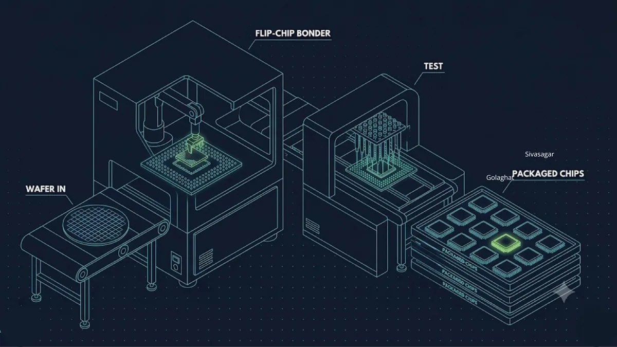
Tata Electronics (TSAT), Jagiroad, Assam is deploying three platform technologies: wire bond, flip chip, and a proprietary multi-die solution called Integrated Systems Packaging (ISP). This is not a wire-bond-only assembly shop. Flip chip is already part of the technology roadmap, and ISP is designed for multi-chip modules used in automotive and AI inference applications. Qualcomm has signed on as a customer for automotive chip modules, and Intel is a named manufacturing client. Pilot production is running as of October 2026, with commercial launch expected between December 2026 and January 2027. Design capacity: 48 million chips per day.
CG Semi (CG Power + Renesas + STARS), Sanand, Gujarat runs an end-to-end OSAT operation: assembly, packaging, testing, and post-test services. The facility handles both traditional packages (QFN, QFP, SOIC, TSSOP, SOP) and advanced formats including flip-chip BGA, CSP, and advanced QFN. Its focus is logic chips for consumer electronics and automotive systems. CG Semi cleared formal customer qualification in roughly 10 months, faster than the Southeast Asian norm. The G1 line has been commercial since July 2026, and the G2 advanced line, targeting end of CY2026, will add flip-chip BGA capability. Peak capacity: ~14.5 million chips/day at full ramp.
Kaynes Semicon, Sanand, Gujarat specialises in Intelligent Power Modules (IPMs), compact integrated assemblies that pack 17 chips per module for applications ranging from ACs and washing machines to EVs and industrial motor drives. Its packaging tiers span QFN/TO (traditional), BGA/FC-BGA (advanced), and 2D/2.5D/3D (commissioning). Kaynes shipped India’s first commercially packaged multi-chip modules to Alpha and Omega Semiconductor in California, and is now commissioning silicon photonics modules and flip-chip BGA lines. Phase 1 capacity: ~1.5 million chips/day, peak target: ~6.3 million chips/day.
Micron Technology ATMP, Sanand, Gujarat was inaugurated on 28 February 2026 and produces DRAM and NAND memory modules and SSDs for computing, AI, and data storage. Wafers arrive from Micron’s global fab network and go through assembly, test, mark, and pack in a cleanroom of approximately 5 lakh square feet. The facility will generate ~5,000 direct jobs when fully operational.
The narrative that India is doing “only basic packaging” is already outdated. Tata Electronics and CG Semi both have flip-chip lines on the floor or in commissioning. Kaynes is working on 2.5D and silicon photonics modules.
For more on what these plants actually consume from a supply chain, see our TSAT Packaging Process and MSME Component Map.
Myth 2: Packaging capacity is abundant and India adds nothing to it
In 2024 and 2025, the single biggest constraint on NVIDIA’s ability to ship H100 and B200 AI accelerators was not wafer fabrication.
It was CoWoS advanced packaging capacity at TSMC.
Epoch AI estimated that the largest AI chip designers used about 90% of global CoWoS capacity and HBM supply in 2025, but only about 12% of advanced logic wafer output. The bottleneck was the backend, not the frontend.
Figure · AI chip supply chain utilisation (2025)
The bottleneck is in packaging and memory, not wafer fabrication.
Key facts:
- TSMC said it was working to double CoWoS capacity
- Nvidia alone was booking roughly 60% of the available CoWoS supply
- Demand exceeded CoWoS supply by an estimated 40-50%, with lead times beyond 40 weeks
- The global OSAT market is a $46 to $50 billion market in 2026, growing at 8-10% a year
India’s current OSAT plants do not operate at the CoWoS frontier. But the OSAT market spans a wide range of packaging technologies from wire-bond to flip-chip to system-in-package. The plants at Sanand and Jagiroad are entering this market at a point when every major chipmaker is looking for geographic diversification in its backend supply chain.
The alternative to adding capacity is not adding capacity. That is not a neutral choice. It means continuing to depend entirely on Taiwan, China, Malaysia, and South Korea for a step in the semiconductor value chain that the AI boom has turned into a chokepoint.
Myth 3: No country ever built a semiconductor industry by starting with packaging
This claim makes the least sense. Consider some of the current leaders in semiconductors.
Taiwan
In the early 1970s, Taiwan already had an established IC packaging industry, heavily dependent on foreign investment and imported components. Texas Instruments and other multinationals set up assembly lines, trained a generation of engineers, and created the workforce known as the “transistor girls.”
The government then channelled that workforce into wafer fabrication through ITRI’s technology transfer programme with RCA. TSMC was founded in 1987, more than fifteen years after the packaging industry had taken root. Taiwan still holds more than half the global market share in semiconductor testing and packaging today.
Malaysia (Penang)
Penang’s semiconductor cluster started in 1972 when Intel, AMD, HP, and five other multinationals set up offshore packaging and assembly operations in a free trade zone. The state government chose the semiconductor backend deliberately because it was labour-intensive and could absorb unemployment quickly.
Fifty years later, the results speak for themselves: Penang contributes approximately 13% of global chip packaging and testing output, GDP per capita runs 34% above the Malaysian national average, and the cluster hosts over 350 multinationals and 4,000 supporting SMEs. Intel has now announced a $7 billion investment to build its largest advanced 3D packaging facility globally in the same Penang it entered as a packaging operation half a century ago.
We wrote a detailed comparison of Penang, Sanand, and Morigaon’s semiconductor packaging clusters earlier this year, mapping what Penang built over five decades, what Sanand is racing to build now, and the 70-point ecosystem readiness gap Morigaon must close.
Figure · From packaging to advanced fabs: how long did it take?
Taiwan, Malaysia, and India. Packaging came first in every case.
Penang is not the story of a country that failed to build fabs and settled for packaging. It is the story of a cluster that started with packaging, built a workforce and supply base over decades, moved up the value chain, and is now the site where Intel is putting its most advanced backend technology.
India is at the start of that curve. The fact that it is at the start is not the same as failure.
What ISM 1.0 actually did
The India Semiconductor Mission was approved by the Union Cabinet on 15 December 2021 with an outlay of ₹76,000 crore. Its first phase, now known as Semicon 1.0 or ISM 1.0, offered 50% fiscal support on project cost for fabs and OSATs. The scheme’s mandate was to get anchor investments on the ground:
| Facility | Location | Investment | Approved | Status (Oct 2026) |
|---|---|---|---|---|
| Micron ATMP | Sanand, Gujarat | $2.75 billion | Jun 2023 | Commercial production |
| Tata-PSMC wafer fab | Dholera, Gujarat | ₹91,526 crore | Feb 2024 | Under construction |
| CG Semi OSAT | Sanand, Gujarat | ₹7,584 crore | Feb 2024 | Commercial production |
| Tata TSAT | Jagiroad, Assam | ₹27,120 crore | Feb 2024 | Pilot production |
| Kaynes Semicon OSAT | Sanand, Gujarat | ₹3,307 crore | Sep 2024 | Commercial production |
Three things the critics routinely miss:
- ISM 1.0 did approve a fab. The Tata-PSMC facility at Dholera is a 28/40nm wafer fabrication plant targeting 50,000 wafer starts per month. It is under construction. The narrative that India approved “only” packaging plants erases a ₹91,000 crore fab from the record.
- Packaging plants came online first because they build faster. A fab takes four to five years from groundbreaking to first silicon. An OSAT can reach commercial production in two to three. Criticising the government for the packaging plants arriving first is criticising physics and construction timelines, not policy.
- The scale is real. Tata’s Jagiroad facility alone is designed for 48 million units per day. CG Power’s OSAT is designed for 15 million units per day. These are not token plants.
For the full fiscal structure behind these approvals, see our Semicon 2.0 Gazette Analysis and Semicon 2.0 Guidelines Rulebook.
India’s OSAT capacity: what the next two years look like
The India Electronics and Semiconductor Association (IESA) projects that national chip production capacity could reach 75 to 80 million units per day by early 2027 as all approved facilities come online. Here is the plant-by-plant build-up:
Figure · India’s projected daily OSAT capacity at full ramp
Plant-by-plant nameplate capacity. Full ramp expected by 2027-28.
Nameplate design capacities at full ramp. Micron Sanand (memory ATMP) not included as its daily output is measured differently. Actual output depends on ramp timing, yields, and customer orders. Sources: Company announcements, PIB, TrendForce.
In 2021, India produced zero semiconductor devices of any kind. By early 2027, cumulative nameplate capacity across these facilities reaches 75 to 80 million chips per day. Tata TSAT alone, at 48 million units per day, would make India a top-20 OSAT site globally by volume, though not yet by revenue or technology tier.
The customer list is already international: Qualcomm and Intel at Tata, Alpha and Omega Semiconductor at Kaynes, Renesas at CG Semi. These are not captive plants running test batches. And the chip types span memory, logic, and power: Micron handles DRAM/NAND, CG Semi handles logic for consumer and automotive, Kaynes builds intelligent power modules, and Tata does automotive and multi-chip modules.
This is diversification from the start, not a single-product bet.
For details on the bill of materials these plants will import (and what India might eventually localise), see our India Semiconductor Input Bill report.
What Semicon 2.0 changes
ISM 1.0 was a fab-first programme: get the anchors on the ground. ISM 2.0 is a broader bet.
The Union Cabinet approved Semicon 2.0 on 15 July 2026 with an outlay of ₹1,27,500 crore, up from ₹76,000 crore in the first phase. MeitY notified the scheme in the Gazette of India on 31 August 2026, and released detailed guidelines on 16 September.
Figure · ISM 1.0 vs. Semicon 2.0: what changed
The shift matters. ISM 1.0 funded the anchors. ISM 2.0 funds the ecosystem around them. The Electronics Component Manufacturing Scheme, expanded to ₹40,000 crore, now targets upstream suppliers of gases, chemicals, lead frames, bonding wire, and cleanroom hardware. The equipment and materials pillar is considering a 12-year incentive window because domestic raw material and equipment suppliers need a longer runway than the anchor plants did.
Alongside the policy, NITI Aayog’s Frontier Tech Hub released a ten-year roadmap targeting a $120 to $150 billion semiconductor value chain by 2035, built on a “More-than-Moore” strategy that concedes leading-edge fabs to Taiwan and Korea and concentrates on mature-node manufacturing, advanced packaging, compound semiconductors, and design.
That strategy is what the industry calls the sweet spot: the range of nodes and technologies where most of the world’s chips are actually manufactured, and where the supply chain gaps are widest.
For a deep dive into every Semicon 2.0 category, capital floor, and MSME angle, see our Semicon 2.0 Gazette Notification Analysis.
What the critics get right
The honest version of the criticism is not that India chose packaging. It is that the current plants are early-stage, the technology is not yet at the advanced packaging frontier, the import dependence is heavy, and the ecosystem is thin.
Those points are valid:
- India’s OSAT plants currently operate on legacy packaging processes, with flip-chip lines still being commissioned
- 60-70% of material inputs are still imported, from lead frames to bonding wire to process chemicals (Swarajya)
- The transition to 2.5D and eventually CoWoS-class packaging is years away
- The local supply base is only beginning to form, as the 600 MSMEs clustering around Sanand demonstrate
- Scale is a real gap: the daily output of CG Semi’s G1 plant is a fraction of what ASE or Amkor produce
- Indian branches of global suppliers tend to price at import parity, tariffs included, which undercuts the localisation case
India is not yet a serious competitor for global OSAT market share. It is a participant, not a leader. But the relevant comparison is not India versus ASE. It is India with these plants versus India without them.
Five years ago, India had zero semiconductor manufacturing capacity of any kind. Today it has three to five plants in commercial or pilot production, a wafer fab under construction at Dholera, a ₹1.27 lakh crore policy framework in Semicon 2.0, international customers placing orders (Qualcomm, Intel, Alpha and Omega Semiconductor, Renesas), a workforce pipeline being trained across the value chain, and an emerging MSME ecosystem of 600-plus firms around Sanand alone.
The baseline was zero. Every unit of capacity above zero is progress.
The Penang lesson
Penang did not become a $75 billion semiconductor export hub by announcing it would build a world-class fab in its first decade. It became one by doing packaging well for long enough that the entire upstream and downstream ecosystem grew around it. The workforce deepened. The SME base diversified. Intel went from an assembly line in 1972 to a design centre in 1992 to the world’s largest advanced 3D packaging facility in 2026.
The lesson is not that India should stop at packaging. It is that packaging is where you start, and the measure of success is not what kind of plant you opened this year but what you build around it over the next twenty.
India’s semiconductor strategy is not the best one imaginable. A government with unlimited political capital, a trained workforce, and $100 billion in patient capital would skip straight to leading-edge fabs. India does not have those things.
What it has is a policy framework, anchor investments, plants that are running, and a second phase that funds the supply chain those plants will need.
That is not all packaging and no chips. That is the foundation being poured.
Related reading from Nitisagar Advisory
- Semiconductor Packaging Clusters in Asia: Penang, Sanand, Morigaon — Comparative ecosystem analysis
- TSAT Packaging Process and MSME Component Map — What an OSAT plant actually consumes
- India Semiconductor Input Bill 2026 — The import bill India will run up as capacity scales
- Semicon 2.0 Gazette Notification Analysis — Every category, capital floor, and MSME angle
- Semicon 2.0 Guidelines Rulebook — The approval clock, capex rules, and lock-in terms
- Japan Vertical Keiretsu and Supplier Base — How Japan built its semiconductor supply chain through tiered suppliers
- Industrial Ecosystems 3: How Penang and Singapore Built a Chip Economy — The fifty-year history behind the Penang packaging cluster
- Ground Report: SEMICON India 2026 — Three days on the exhibition floor