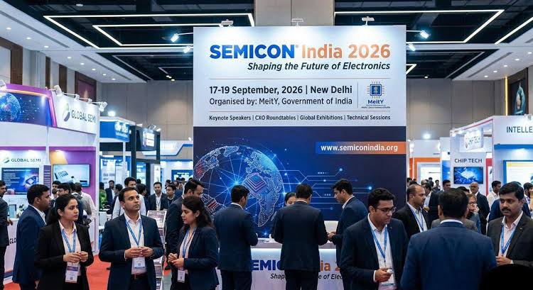
I just got back from three days at SEMICON India 2026 at Yashobhoomi in Dwarka, and the revelation was not at the front of the hall.
The front of the hall was, as everyone expected, the household names. ASML’s booth was a queue. Tokyo Electron had a stage. Fujifilm, Applied Materials, the Tatas. Tour groups moved between them in a slow, dutiful rotation. The Prime Minister had inaugurated the show two days earlier and MeitY minister Ashwini Vaishnaw had done the ribbon on the state pavilions. You can read that part of the event in any wire report.
The revelation was in the smaller booths. About 500 exhibitors turned up over three days, and for every ASML there were ten companies whose annual sales top out somewhere between ten and fifty million dollars. Gas suppliers. Valve makers. A Taiwanese outfit that only sold anti-static plastic cases for wafer transport. A Singaporean firm that does one specific class of ultra-pure quartz component. A Malaysian family business, second generation, that started out fabricating stainless tubing for petrochemicals and now sells to two of the OSATs going up in India.
Those were the booths I spent my three days at. Because that is the ecosystem, and the ecosystem is the story.


Why the small booths matter
The reason I went to Yashobhoomi was not to gawk at lithography machines. It was to answer a question we get asked constantly at Nitisagar: what does an MSME in Assam actually build for a semiconductor plant?
The honest answer, from the floor, is: many more things than the term “high-tech” suggests. Chips themselves are science fiction. The lifecycle around them is, for the most part, normal industrial work done to unusual specifications. Tubes and valves. Ultra-pure gases and process chemicals. Filters. Coatings. Anti-static plastic packaging cases. Metrology fixtures. The small components run into the hundreds, and each is unremarkable in isolation. Put three hundred of them together in one industrial estate and you have what Taiwan, Malaysia, and now Vietnam have: a functioning supply base that will still be there when the next generation of fabs comes.
That is what we are trying to seed in Assam. I’ve written before about what the Jagiroad OSAT actually needs from an MSME supply chain and about the input bill India will run up as capacity comes on. SEMICON India is where I got to test those hypotheses against real suppliers with real order books.
Five observations from the floor.
1. Not every component is high-tech
Walking the small-supplier rows, the pattern was consistent. A large share of what a fab or an OSAT consumes is refined, customised, quality-controlled industrial hardware, not exotic technology. A high-purity nitrogen line. A pneumatic valve rated for a specific chemistry. A vacuum bellows with a documented life of 200,000 cycles. A plastic wafer-carrier case moulded to a tolerance and treated to bleed static.
The specifications are exacting. The underlying manufacturing is not. Hold tolerance, document your process, pass a customer audit, and you can play here. Our own report on the certification stack a Northeast MSME actually needs is the operational corollary. Certifications turn an ordinary competent workshop into a qualified supplier.
The Assam MSMEs I keep in touch with are not going to make lithography optics. What they can build, today, at Rs 1.5-15 crore of entry capex:
- Gas cabinets and gas-line hardware
- Cleanroom furniture and HDPE / PP piping
- Anti-static packaging and wafer-transport cases
- Consumable filters and metrology fixtures
That range sits squarely inside what our Incentive Estimator is scoped to.
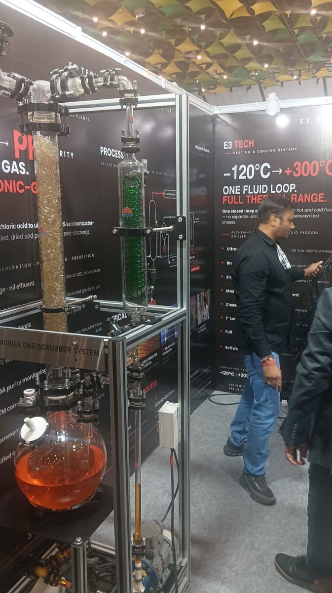
2. Machines are only one part of the story
Every capital piece of equipment on that floor came with an unglamorous shadow: service.
The machines are largely automated. What they need, and what an Indian ecosystem currently under-supplies, is a workforce that can plug a laptop into the diagnostic port, read the fault log, predict the failure (a bellows nearing its 200,000-cycle life, a pump seal running warm), then physically take the sub-assembly apart and replace the worn component. That is service engineering. It is a career. It does not require a PhD and it is not getting automated any time soon.
Sitting alongside that is the entire techno-legal layer: certification, metrology, calibration, compliance, audit, accreditation. You don’t need to be an operator or a designer to make a living here. You need to understand how industrial processes and complex supply chains actually work, and you need paperwork that a Fortune-500 customer’s procurement office can accept. Half a functioning ecosystem is that paperwork.
3. Most MSMEs started off doing something else
This one I was not prepared for.
Booth after booth of Japanese, Singaporean, Taiwanese, and Malaysian small suppliers had the same origin story. They did not start in semiconductors. They started in pharma packaging. In automotive castings. In petrochemical piping. In stainless tubing for food processing. Semiconductors matured, and the industrial muscle memory these companies had built up over decades in adjacent industries turned out to be transferable. Precision, cleanliness, documentation, audit-readiness: those competencies do not care what your first customer was.
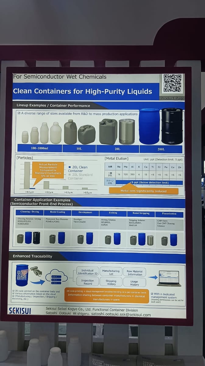
I met Indian companies with the same trajectory. A Gujarat outfit that has laid corrosion-resistant coatings on petrochemical piping and refinery infrastructure for thirty-plus years now ships to semiconductor fab customers. A Chennai family firm that started with automotive-grade fasteners in the eighties is now qualifying parts for one of the ATMP lines coming up in Sanand. Zoom out one level and you get Rajkot’s engineering cluster, where 10,000 small units that started copying oil engines in the 1950s now cast and machine to European automotive tolerances. Whole clusters can pivot upwards, not just single firms.
The lesson for an Assam MSME founder is important and, I think, freeing: you do not have to wait for the semiconductor economy to arrive to start building the muscle. If you already make something to a documented spec (pharma-grade fittings, food-contact plastics, precision castings for automotive), the transition to semiconductor-grade work is a matter of certifications, process controls, and customer qualification cycles. Not a rebirth.
This is why we have spent so much time on the Japan vertical keiretsu supplier base and the Japan industrial resilience playbook. The Japanese suppliers on the SEMICON floor are the endgame version of exactly this pattern.
4. Government alignment can be a powerful thing, when it shows up in one place
The government was not decorative at SEMICON. It was operational.
MeitY had a large stand. The India Semiconductor Mission, the agency running the Rs 1.2 lakh crore programme, had a bigger one. Seven or eight state pavilions were present in force: Karnataka, Tamil Nadu, Uttar Pradesh, Odisha, Gujarat, Maharashtra, Andhra Pradesh, and Assam, which stood up creditably against pavilions with much bigger budgets.
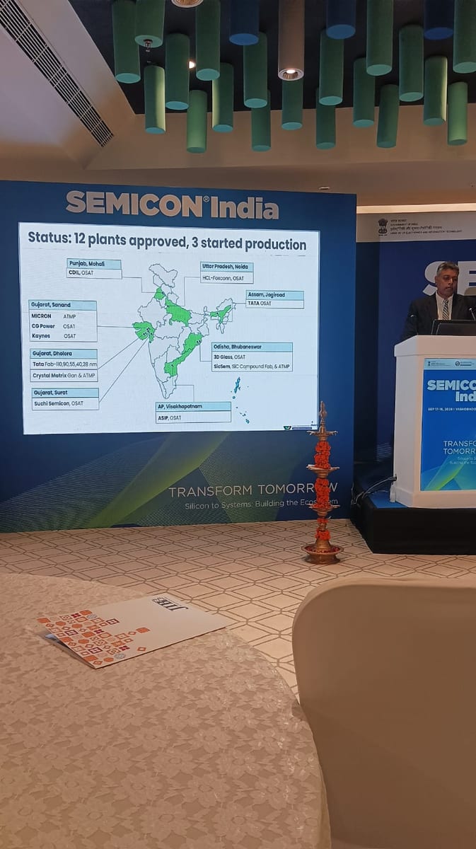
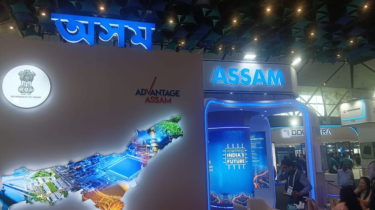


At Nitisagar Advisory we’ve mapped Assam’s own stack in the Assam Industrial Policy Explorer. Seeing peer states pitch their own alongside ours widens the ecosystem. A whole-of-country approach is exactly what the supplier base needs.
The most useful hours of my three days was a session organised by JIBB on India-Japan semiconductor cooperation, part of the SEMICON Setu track. That partnership is where a lot of the Assam story eventually lands, and Japan Calling has the fuller readout from the room: Building the bridge, India-Japan semiconductor cooperation at SEMICON Setu 2026. My own notes went up on LinkedIn straight after.
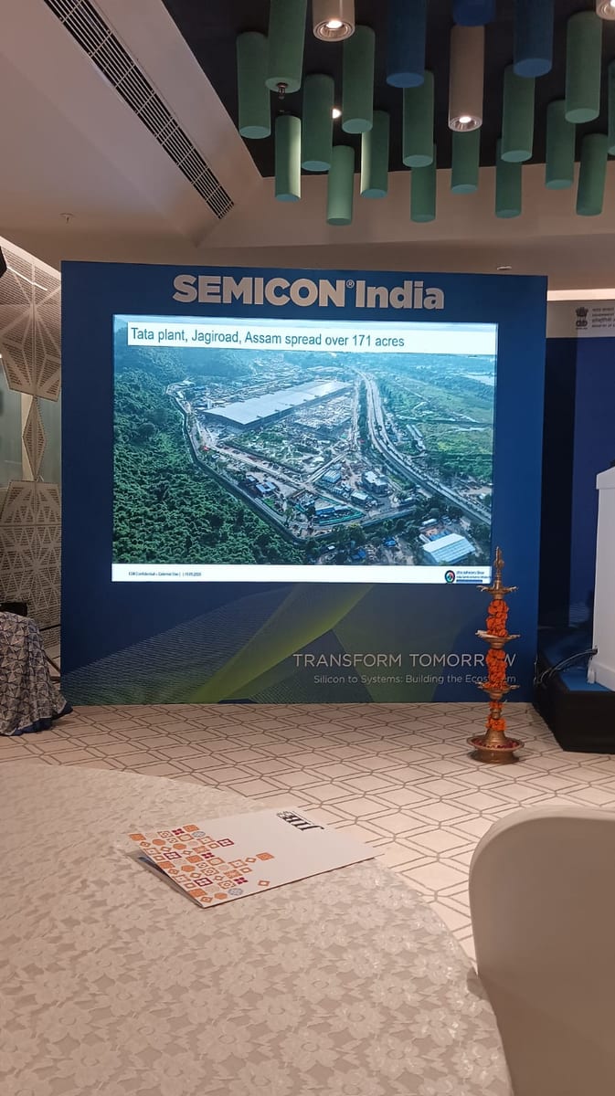
Two things stood out from the government footprint overall. States are competing on incentive design now, which is healthy: anchor investors have real options, not a pre-selected destination. And the ISM presence is operational, not evangelical.
That is a shift from two years ago.
5. Academia and talent development didn’t skip the party
The last thing I did not expect at the scale I saw was the academic footprint. IIT Delhi, IIT Bombay, IISc, and a slew of public and private institutions, a cluster of state-supported VLSI design centres were present. I also met institutes running training courses for cleanroom operators, precision machinists, metrology technicians etc. that Semicon 2.0’s talent-development pillar is designed to fund through the ISM portal.
You cannot run a semiconductor ecosystem without the human pipeline, and the pipeline was on the floor.
What I am taking home
Three days at Yashobhoomi did not change my thesis. It confirmed it. The Indian semiconductor story is being sold as fabs and anchor investments and headline numbers, and that is understandable. Fabs win press cycles. But the beating heart of any semiconductor economy is a dense, boring, competent tier 3 and tier 4 supplier base. Hundreds of firms doing unglamorous things well, with the paperwork to prove it.
For Assam, that base does not yet exist at scale. We will build it one MSME at a time, one certification at a time, one qualified shipment at a time. The supply-chain map we maintain and the component-level breakdown we published in August are our first passes at showing founders where their entry points are. SEMICON India was a three-day, in-person confirmation that the entry points are real.
If you were on the floor and we did not manage to meet, or if you are a Northeast MSME founder trying to figure out which of these openings is yours, you know where to find me.
A ground report from Yashobhoomi, Dwarka, 17-19 September 2026.