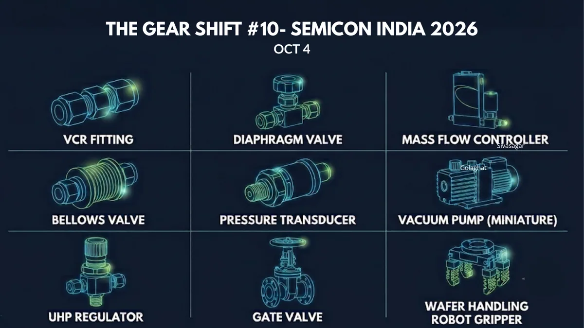
The Prime Minister opened SEMICON India 2026 at Yashobhoomi on 17 September and put ISM 2.0’s price tag at $13.5 billion. Five semiconductor plants are in commercial production. Applied Materials, Lam Research, and Fujifilm committed a combined ₹1.44 lakh crore the same week. Tata’s Jagiroad OSAT is packaging chips ahead of its December commissioning date. Eight states brought pavilions and chequebooks.
I was on the floor for three days and wrote a ground report on the supplier ecosystem I went looking for. This issue of Gear Shift is the policy and business companion to that report: ten stories from in and around SEMICON India, read through the lens of what they mean for an MSME founder trying to figure out where the entry points are.
This is a special edition, twice the usual length. Pour the chai.
Story 1: ISM 2.0 Gets the Cabinet Nod, and the PM Opens the Show with $13.5 Billion
The India Semiconductor Mission’s second phase was announced in Budget 2026 on 1 February and received full cabinet approval on 15 July with an outlay of ₹1,27,500 crore, up from ₹76,000 crore in the first phase. Prime Minister Modi used the SEMICON India 2026 inaugural on 17 September to frame the number for a global audience: $13.5 billion.
ISM 1.0 was a fab-first programme - get the anchor investments on the ground, worry about the ecosystem later. ISM 2.0 is built around six pillars: chip design, semiconductor equipment and materials, fabrication, advanced packaging, applied R&D, and talent development. Two of those six - equipment and materials, and design - had no dedicated central spending line until this year.
The equipment and materials pillar is the one to watch. The government is weighing a 12-year incentive window for ISM 2.0, specifically because domestic raw material and equipment suppliers need a longer runway before they can compete at global scale.
The MSME angle: ISM 2.0 is the programme that creates your funding line. ISM 1.0 funded fabs and OSATs. ISM 2.0 funds the companies that supply them. The Electronics Component Manufacturing Scheme, now expanded to ₹40,000 crore, targets exactly this upstream layer. If you make anything from high-purity gas fittings to cleanroom hardware to anti-static packaging, the central incentive stack is no longer designed only for the anchor - it is designed for you.
Story 2: Applied Materials Commits $5 Billion Through India Vision 2035
Applied Materials, the world’s largest semiconductor equipment maker by revenue, announced India Vision 2035 at SEMICON India: $5 billion over the next decade, anchored by a 140-acre advanced semiconductor research park with cleanroom capability, engineering teams, and collaborative R&D on one site.
The supply chain number matters more than the research park: Applied Materials wants to grow its India-based supply chain capacity tenfold by 2035.
The MSME angle: Tenfold capacity means tenfold the number of Indian firms Applied Materials buys from. Its procurement is audit-heavy, qualification-heavy, documentation-heavy, but the bar is ISO plus customer-specific quality management. The certification stack we have mapped for Northeast MSMEs is the starting line.
Story 3: Lam Research Bets ₹10,000 Crore on India’s First Silicon Component Facility
Lam Research announced on 16 September that it will invest approximately ₹10,000 crore to build India’s first silicon component manufacturing facility, alongside expanded R&D in Bengaluru. The facility covers a vertically integrated process from silicon ingot production through processing.
Between Lam, Applied Materials, and Fujifilm, the three days around the show saw combined India commitments worth ₹1.44 lakh crore. All three are equipment and materials companies. That is not a coincidence - it is a direct response to ISM 2.0 creating a dedicated spending line for the upstream supply chain.
The MSME angle: No MSME competes with Lam’s vertically integrated process. But every such facility needs local services: precision machining for jigs and fixtures, industrial gas supply, logistics, facility management, cleanroom consumables. When the location is announced, it defines a new catchment for the kind of MSME service provider I spent three days talking to at Yashobhoomi.
Story 4: Fujifilm Plants ₹800 Crore at Dholera for Semiconductor Chemicals
Fujifilm announced a greenfield semiconductor materials manufacturing facility at Dholera SIR, Gujarat, total investment around ₹800 crore:
- Phase 1: front-end process chemicals.
- Phase 2: semiconductor surface conditioning materials and high-purity chemicals.
- Commercial production targeted for fiscal year 2028.
This is the industrial chemicals division that supplies the wet-processing fluids semiconductor fabs use to etch, clean, and condition wafers. India currently imports almost all of these. Fujifilm’s facility will be among the first to manufacture them domestically under ISM 2.0’s materials pillar.
The MSME angle: Process chemicals are consumables: used up and re-ordered every production cycle. The supply chain around Dholera will need bulk raw materials, ultra-pure water systems, specialised packaging (exactly what I described in my ground report covering the Sekisui booth), and logistics that maintain purity during transport. Indian chemical MSMEs who already serve pharma or petrochemicals to documented purity standards are the natural candidates.
Story 5: Five Plants Are Now in Commercial Production
This is the headline most of the wire coverage missed, because it happened gradually and no one rang a bell. As of SEMICON India 2026, five semiconductor plants in India are in commercial production, out of twelve approved under ISM 1.0.
The scorecard:
- Micron, Sanand: opened February 2026. India’s first commercial semiconductor assembly and test facility. $2.75 billion investment, 500,000+ sqft of cleanroom. Assembling and testing tens of millions of DRAM and NAND chips, scaling to hundreds of millions in 2027. Shipped its first made-in-India memory modules to Dell.
- CG Semi, Sanand: launched commercial production at its G1 OSAT on 4 July 2026. ₹7,600 crore investment. Currently at 200 million chips per year, targeting 5 billion chips annually at full capacity.
- Kaynes Semicon, Sanand: commercial production by March 2026, just 14 months after breaking ground. Shipped India’s first commercially produced 900 multi-chip modules and is scaling to 6.3 million chips per day.
Two more are in production elsewhere. The remaining seven are under construction.
The MSME angle: Commercial production means active procurement cycles. These are plants ordering consumables, replacement parts, service contracts, and logistics on a recurring basis. The time to be pursuing a supplier audit is now, not when all twelve are running. Our component-level breakdown maps where those orders land.
Story 6: Tata OSAT at Jagiroad, Where Assam Enters the Map
Tata Electronics’ ₹27,120 crore OSAT facility at Jagiroad, Morigaon district, is the reason Assam appears on the ISM status slide I photographed at SEMICON India.
The timeline as of September 2026:
- A team from the Karnataka unit relocated to Jagiroad by end of May to oversee technology transfer.
- One complete production line moved from Tata’s Vemagal facility to begin operations ahead of schedule. Chip packaging is underway in Assam today.
- Full plant commissioning targeted for December 2026.
- Full capacity: 48 million chips per day, the largest OSAT in India and Southeast Asia.
At SEMICON India, the CM urged investors to tap semiconductor opportunities in the state. The ecosystem around Jagiroad:
- ASMPT, DISCO, Besi, Cadence, and Tokyo Electron have set up operations in Assam.
- Tata Group signed agreements with two additional semiconductor firms.
- Employment projection: more than 15,000 direct and 11,000-13,000 indirect jobs.
The MSME angle: This is the anchor that decides whether a semiconductor supply chain takes root in Northeast India or stays a Gujarat-and-south story. ASMPT, DISCO, Besi, and TEL do not set up operations in a state where they expect the plant to stall. With chip packaging already underway, the vendor qualification window is not December onwards. It is now. The supply-chain map and OSAT component breakdown show where those orders land. The plant has since produced its first pilot chips, covered in Issue #11.
Story 7: Tokyo Electron Partners Tata, and the Japan Corridor Gets Real
Tokyo Electron, Japan’s largest semiconductor equipment maker, signed an MoU with Tata Electronics to supply equipment and services for both the Dholera fab and the Jagiroad OSAT. The partnership covers front-end fabrication and back-end packaging technologies, plus workforce training and joint R&D.
The MoU came in the same month as the largest-ever Indian business delegation to Japan and a cabinet-approved memorandum of cooperation between India and Japan on semiconductor supply chains. The most useful session I attended at SEMICON India was organised by JIBB on India-Japan semiconductor cooperation. The slide on stage showed the Tata plant at Jagiroad, spread over 171 acres.
The MSME angle: The Japan corridor is not abstract for Northeast India. The Japan vertical keiretsu supplier base report maps how Japanese supply chains work, and the Japan industrial resilience playbook shows what Assam can learn. TEL at Jagiroad means Japanese qualification standards in Morigaon district. An MSME that can pass a Japanese customer audit (documentation-heavy, process-heavy, relationship-heavy, but not technology-impossible) is positioned for the highest-value tier of the supply chain.
Story 8: 200 Chip Design Startups, and the Scheme Nobody Talks About
The hardware announcements took the headlines. The design side of ISM has been building underneath. At least 200 chip design companies have emerged under ISM, and the Design Linked Incentive scheme has delivered:
- 105 startups with access to EDA tools.
- 20 with venture capital funding.
- Multiple tape-outs and patents.
The DLI scheme offers up to ₹15 crore in product development support and 6-8 per cent of net sales for five years. It is designed for startups and MSMEs, not for Tata-scale players.
The MSME angle: Every chip design company that completes a tape-out needs packaging, testing, and validation services. The 200 design startups emerging from the DLI pipeline will not all build their own test infrastructure. They will outsource it to the same OSAT ecosystem that ISM 1.0 funded. As that ecosystem grows, so does the need for PCB fabrication, prototype packaging, test fixture manufacturing, and engineering services that a ₹2-15 crore MSME can provide.
Story 9: The States Are Jousting, and Assam Just Put ₹25,000 Crore on the Table
Eight state pavilions lined the aisle at SEMICON India. What was on display was not tourism. It was a live incentive-design competition. Two states did something genuinely interesting for MSMEs.
Gujarat has the lead with capital subsidies of up to 40 per cent over and above central incentives. Sanand is already home to Micron, CG Semi, and Kaynes. Dholera has the Tata fab and Fujifilm’s chemicals facility. Tamil Nadu has launched the Tamil Nadu Semiconductor Mission 2030 with a 50 per cent state top-up and five pillars covering design firms, testing, centres of excellence, equipment parks, and workforce training.
Then there is Odisha, which did something no other state has. Its third amendment to the semiconductor policy added 25 per cent additional capital support for ISM-approved projects, and extended the policy scope beyond traditional semiconductor manufacturing to include equipment production, semiconductor-grade chemicals, specialised gases, and advanced materials. Odisha became the first state to offer dedicated policy support for the semiconductor supply chain, not just the anchor plant. It has already attracted proposals worth ₹23,600 crore.
And then there is Assam. At a Delhi roundtable with industry leaders after SEMICON India, CM Sarma announced that Assam has earmarked ₹25,000 crore in incentives for semiconductor and electronic component manufacturers, offering 60 per cent additional incentives on top of central government support plus GST rebates and power ecosystem development. His claim: Assam has the best semiconductor policy in the country, better than Gujarat, Tamil Nadu, or any other state.
The argument, stripped of the politics, is arithmetic. Assam’s 60 per cent state top-up beats Tamil Nadu’s 50 per cent and Odisha’s 25 per cent on paper. Any company setting up an electronic components unit in Assam stacks two programmes: the central ECMS and Assam’s own state semiconductor policy. The old northeast-specific UNNATI scheme, which would have added a third layer, is no longer accepting applications. Its Assam allocation was exhausted and the portal is closed. So the triple stack the CM’s advisors may be counting is now a double stack, but at 60 per cent the state top-up alone is still the most generous in the country.
The MSME angle: Here is the honest comparison. Odisha’s policy is smarter: it explicitly names the supply chain layers (equipment, chemicals, gases, materials) and creates a dedicated funding line for each. Assam’s headline number is bigger, but the notification does not yet break the ₹25,000 crore down by segment. For a ₹5 crore component maker choosing between Assam and Odisha, the question is not which state has the bigger number but which state has the more navigable application process. As of today, Odisha’s policy is more specific about what qualifies and how to apply. Assam has the anchor (Jagiroad), the proximity advantage, and the larger top-up percentage, but it needs to publish the operational detail that turns a headline number into something an MSME can actually claim. Run the comparison in the Subsidy Calculator and use the Policy Explorer to track when the notification lands.
Story 10: The Talent Pipeline, One Lakh More Engineers, and Who Will Train Them
Semicon 2.0 will train another 1,00,000 semiconductor engineers on top of the 85,000-plus already qualified in four years. The government has trained more than 100,000 engineers overall, with partnerships with Lam Research, IBM, Purdue University, and Arizona State University enhancing skilling and R&D.
The academic presence at Yashobhoomi was larger than I expected: IIT Delhi, IIT Bombay, IISc, and over a dozen other institutions, alongside VLSI design centres and institutes running training courses for cleanroom operators, precision machinists, and metrology technicians. The global chip industry faces a shortage of roughly one million workers by 2032. Semicon 2.0’s talent pillar is designed to fund exactly these programmes through the ISM portal.
The MSME angle: Training is an MSME opportunity, not just an MSME need. Assam has IIT Guwahati, three engineering colleges with VLSI depth, and a rising ITI network. Any Northeast training vendor, industrial skilling firm, or campus placement operator that can credibly deliver even fifty chip-qualified engineers a year is in a market whose central spending line has been raised, not cut. I made this case in Issue #9 and the SEMICON floor confirmed it: the talent-development window on the ISM portal is where a ₹2-15 crore skilling operator can compete. IIT Guwahati and Tata Electronics have since signed a semiconductor packaging Centre of Excellence, covered in Issue #11.
Gear Shift is a fortnightly roundup of India’s manufacturing and industrial policy developments, with a focus on implications for MSMEs in Northeast India. This is a special SEMICON India edition with ten stories instead of the usual five. Published by Nitisagar Advisory, Guwahati.
Read the companion piece: Ground Report: SEMICON India 2026, and the Suppliers I Went Looking For.
If you found this issue useful, subscribe below to receive the next one in your inbox.